Home
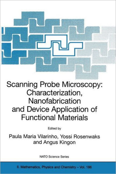
Scanning Probe Microscopy: Characterization, Nanofabrication and Device Application of Functional Materials: Proceedings of the NATO Advanced Study Institute on Scanning Probe Microscopy: Characterization, Nanofabrication and Device Applicatio / Edition 1
Loading Inventory...
Barnes and Noble
Scanning Probe Microscopy: Characterization, Nanofabrication and Device Application of Functional Materials: Proceedings of the NATO Advanced Study Institute on Scanning Probe Microscopy: Characterization, Nanofabrication and Device Applicatio / Edition 1
Current price: $329.99

Barnes and Noble
Scanning Probe Microscopy: Characterization, Nanofabrication and Device Application of Functional Materials: Proceedings of the NATO Advanced Study Institute on Scanning Probe Microscopy: Characterization, Nanofabrication and Device Applicatio / Edition 1
Current price: $329.99
Loading Inventory...
Size: OS
*Product Information may vary - to confirm product availability, pricing, and additional information please contact Barnes and Noble
As the characteristic dimensions of electronic devices continue to shrink, the ability to characterize their electronic properties at the nanometer scale has come to be of outstanding importance. In this sense, Scanning Probe Microscopy (SPM) is becoming an indispensable tool, playing a key role in nanoscience and nanotechnology. SPM is opening new opportunities to measure semiconductor electronic properties with unprecedented spatial resolution. SPM is being successfully applied for nanoscale characterization of ferroelectric thin films. In the area of functional molecular materials it is being used as a probe to contact molecular structures in order to characterize their electrical properties, as a manipulator to assemble nanoparticles and nanotubes into simple devices, and as a tool to pattern molecular nanostructures. This book provides in-depth information on new and emerging applications of SPM to the field of materials science, namely in the areas of characterisation, device application and nanofabrication of functional materials. Starting with the general properties of functional materials the authors present an updated overview of the fundamentals of Scanning Probe Techniques and the application of SPM techniques to the characterization of specified functional materials such as piezoelectric and ferroelectric and to the fabrication of some nano electronic devices. Its uniqueness is in the combination of the fundamental nanoscale research with the progress in fabrication of realistic nanodevices. By bringing together the contribution of leading researchers from the materials science and SPM communities, relevant information is conveyed that allows researchers to learn more about the actual developments in SPM applied to functional materials. This book will contribute to the continuous education and development in the field of nanotechnology.
